Analog Integrated Systems
Experimenting and Learning
Feel free to contact me if you don't understand anything
This project is maintained by HishamElreedy
اللهم لا علم لنا الأ ما علمتنا به انك انت علام الغيوب
PLL Project
Theoretical Part:
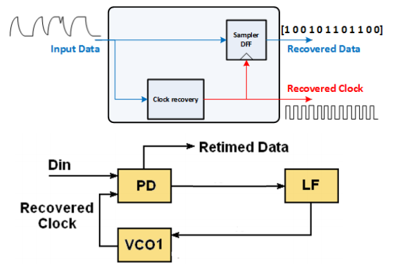
a)what is the application of Clock and Data Recovery (CDR) circuit?
Describe briefly how to use PLL in CDR Applications
Clock recovery is the process of extracting timing information from a serial data stream to allow receiving circuit to decode the transmitted symols. Clock recovery from the data stream is expedited by modifying the transmitted data where in serial communication channel doesn't transmit the clock signal along with the data stream, the clock must be regenerated at the receiver using the timing information from the data stream
- The CDR recovers the exact timing of the incoming data
- The recovering timing is utilized to sample the data at the optimum time
- CDR minmizes jitter of the input signal
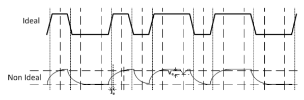
- Due to TX and channel non-idealitieis signal integrity is compromised at the RX input
- Non-idealities in data transition time is defined as excess phase (or jitter)
- The clock and data recovery (CDR) system is reponsible for dealing with jitter
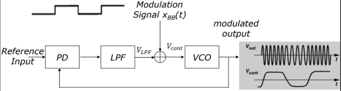
b)Describe briefly how to use a PLL in modulation/demodulation applications
Demodulation of frequency modulation (FM): If PLL is locked to a FM signal, the VCO tracks the instantaneous frequency of the input signal. The filtered error voltage which controls the VCO and maintains lock with the input signal is demodulated FM output. The VCO transfer characteristics determine the linearity of the demodulated out. Since the VCO used in an integrated-circuit PLL is highly linear, it is possible to realize highly linear FM demodulators.
c)Describe briefly the operation of a Delay Locked Loop (DLL)
and mention the advantages & disadvantages compared to a PLL.
Delay locked loop is used to synchronize signal that is spreaded using Direct-Sequence Scheme where we also replaces the internal Voltag-Controlled-Oscillator, by a delay ine. and we use DLL to change the phase of clock signal and also to use it in clock recovery
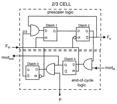
d)Show the schematic of a dual-modulus (2/3) divider.
Hint: This is composed of a divide-by-2 and a divide-by-3 circuits.
Simulate the divider in both modes using ideal logic (using Cadence).
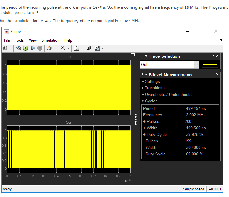
A 2/3 divider cell comprises two functional blocksThe prescaler logic block divides \(F_{in}\), upon control by the end-of-cycle logic, the frequency of the input signal either by 2 or by 3, and outputs the divided clock signal to the next cell in the chain The end-of-cycle logic controls the momentaneous division ratio of the cell. The division ratio depends on the state of \(mod_{in}\) and p signals,The\(mod_{in}\) signal becomes active once in a division cycle. At that moment, the state of the p input is checked, and if p=1 the end-of-cycle logic forces the prescaler to swallow one extra period of the input signal. In other words, the cell divides by 3. If p=0, the cell stays in division by 2 mode. Regardless of the state of the p input, the end-of-cycle logic reclocks the \(mod_{in}\) signal, and outputs it to the preceding cell in the chain
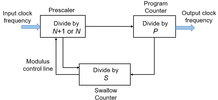
Simulation didnot work well in cadence so I made it in simulink with the following block diagram
The Dual Modulus Prescaler subsystem block consists of a program counter, a swallow counter and a prescaler.
When the block first receives an input signal, the pulse swallow function is activated. The prescaler divides the input signal
frequency by (N+1), where N is defined by the Prescaler divider value (N) parameter.
Both the program and swallow counters start counting. The swallow counter resets after counting to S pulses,
or (N+1)S cycles, where S is defined by the Swallow counter value (S) parameter.
Then, the pulse swallow function is deactivated, and the prescaler divides the input frequency by N.
Since the program counter has already sensed S pulses, it requires (P-S) more pulses, or (P-S)N cycles to reach overflow,
where P is defined by the Program counter value (P) parameter. The cycle repeats after both counters are reset.
$${{f_{in}}\over{f_{out}}}=(N+1)S+N(P-S)=NP+S={2 \over 3}$$
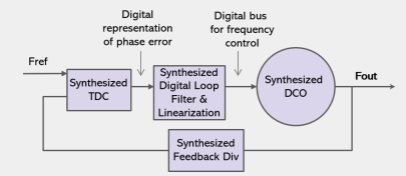
e)What is an all-digital PLL (ADPLL)?
Show the block diagram and the main building blocks
all-digital PLL has all digital elements, including the phase detector, loop filter and oscillator; they don't have the supply limitations of analog PLL ands and advanced all digital phase locked loops are fully synthesizable and customizable. each elements we were designing in analog pll we connect it to ADC and DAC inorder to control it digitally
Simulation Part:
The purpose of this part is to simulate the (linear) PLL circuit in Simulink environment. As discussed in the lecture, the PLL is widely employed in communication and electronic application as it has many functions. In this project, you are going to simulate the PLL as a circuit that performs synchronization between two signals that have different phase and frequency.
Question 1,2,3
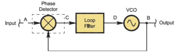
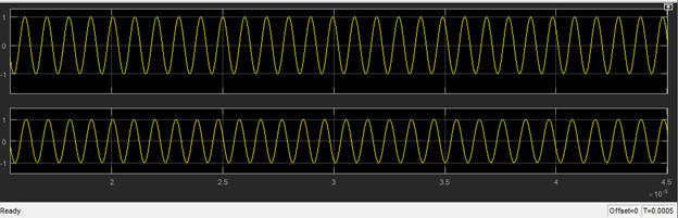
The type of PLL shown in fig(2) is linear model for PLL where, The Model in Figure 2 has three main components:
- The phase frequency detector (PFD):identify phase shift between reference signal
- The loop filter (LF):it is the controller of the PLL which takes voltage input from detector to generate required signal for VCO
- The voltage controlled oscillator (VCO):Generates oscillating frequency according to dc voltage input
- The oscillator: the signal generator that generates the sinusoidal signal we want to synchronize with
- The scope: a visualization block that displays the signal with time
Question 4,5,6
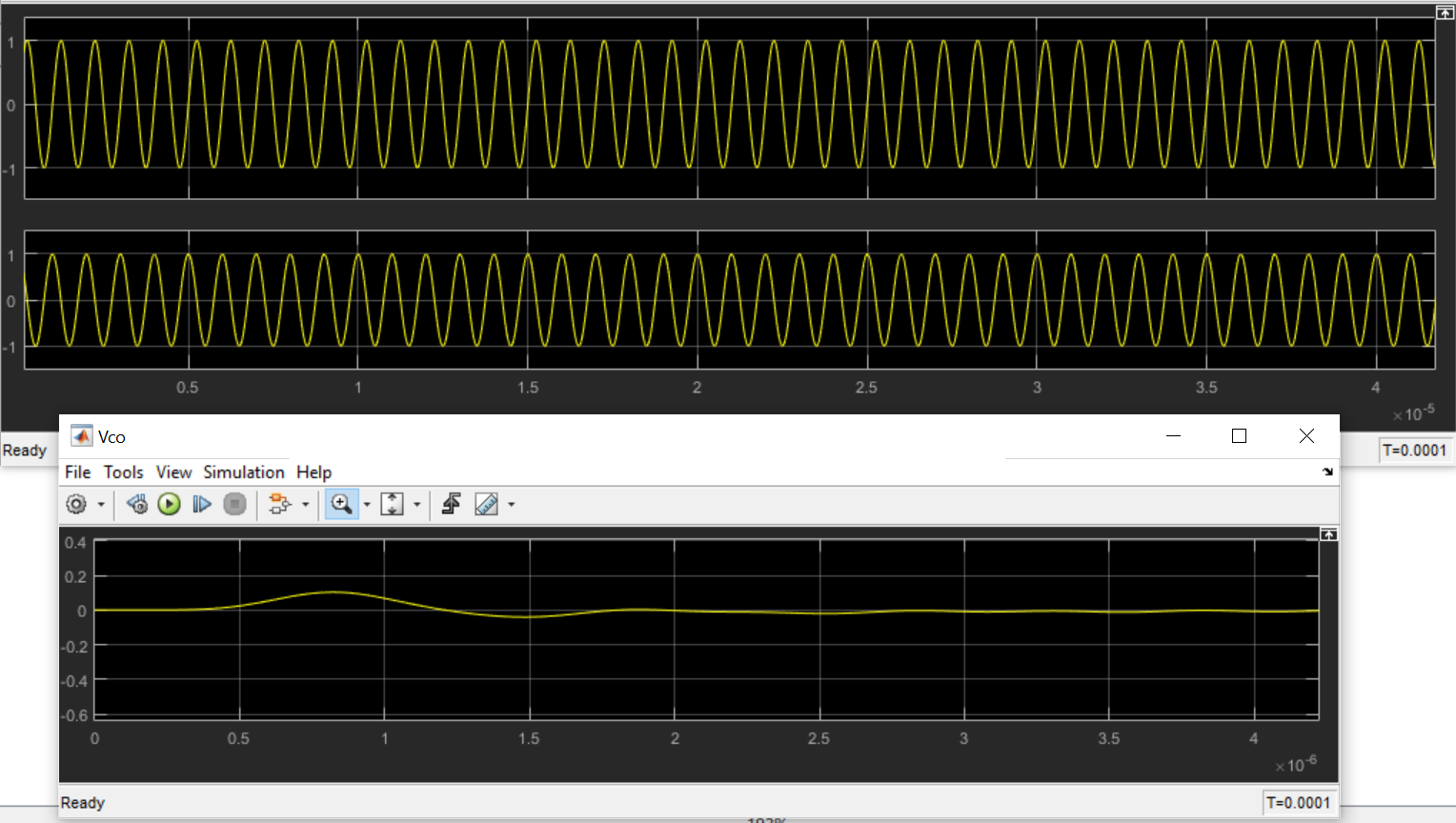
Question 4
- The input is a sinusoidal with frequency of \(10^6Hz\) and zero initial phase
- The VCO has a free running code of \(10^6 Hz\) and gain \(K_{VCO}\) of \(10^5\)Hz/Volt
- The low pass filter has a pass-band edge frequency \(10^6\)Hz, order 7, and Butterworth type
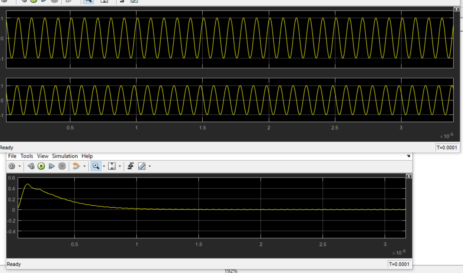
Question 5
- Repeat Question 4 with the following setup change:
- The input is sinusoid with frequency equal to \(10^6Hz\) and phase shift of \(\pi \over 3\)
Question 6
- The input is a sinusoidal with a frequency equal to \(10^6\) and initial phase shift of \(\pi \over 5\)
Question 7&8&9
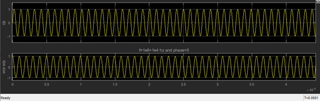
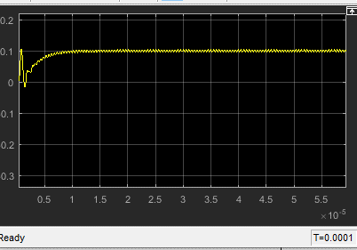
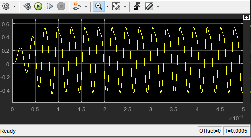
Question 7
Testing the circuit after making:
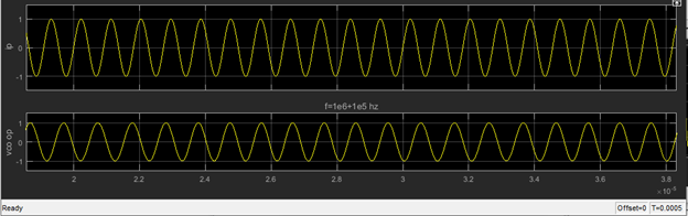
- The input is sinusoid with frequency equal to \(10^6+10^4\)Hz and 0 initial phase
- The input has a free running frequency of \(10^6\)Hz and gain \(K_{VCO}\) of \(10^5\)Hz/Volt
- The low pass filter has pass-band edge frequency of \(10^6\)Hz, order 7 and Butterworth type
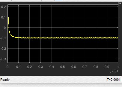
Question 8
Repeat Question 7 with the following setup change:
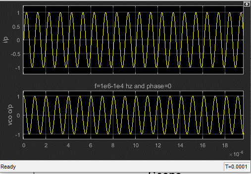
- The input is a sinusoid with frequency equal to \(10^6 - 10^4\)Hz and 0 initial phase
Question 9
Repeat Question 7 with the following setup change:
- The VCO has a free running frequency of \(10^6\)Hz and gain \(K_{VCO}\) of \(2*10^5\)Hz/Volt
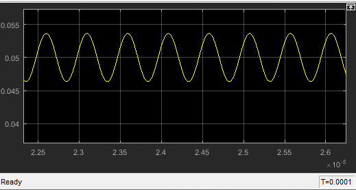
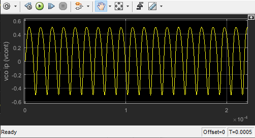
$$\phi_e={{\omega_{out}-\omega_o}\over{K_{PD}*K_{VCO}}}$$ $$VCO_{out}=K_{PD}*\phi_e$$ $$\omega_{out}=\omega_o + K_{VCO}*VCO_{out}$$ the filter in 7,8,9 will settle at 0.1, -0.1 and 0.05 Volts respectively with some ripples $$Case7:\space \phi_e={{\pi \over 2}+\Delta \phi}$$ $$Case8:\space \phi_e={{\pi \over 2}-\Delta \phi}$$ $$Case9:\space \phi_e={{\pi \over 2}+{{\Delta \phi}\over 2}}$$ Increasing VCO gain decreases SS value of the filter as the filter will need less voltage to achieve required F lock
Question 10
Repeat Question 7 with the following setup change:
- The low pass filter has pass-band edge frequency of \(10^5\)Hz, order 7 and Butterworth type
- Output doesn't lock to the input
- \(\tau={1\over{\zeta \omega_n}}={2\over{\omega_{LPF}}}\), then if \(\omega_{LPF}\) decreases, \(\tau\) increases, speed decreases and then stability decreases.
- \(VCO_{out}\) is critically stable
- \(\phi_e\) will be changed in a specific range
Question 11
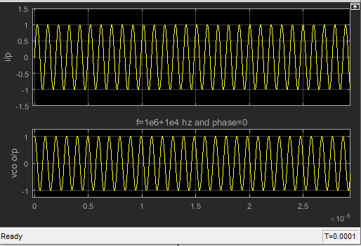
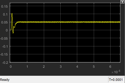
Repeat Question 7 with the following setup change:
- The input is a sinusoid with frequency \((10^6 + 10^5)\)Hz and 0 initial phase