AnalogDesign
Experimenting and Explaining Analog_IC_Design
Feel free to contact me if you don't understand anything
This project is maintained by HishamElreedy
اللهم لا علم لنا الأ ما علمتنا به انك انت علام الغيوب
0. Introduction

0.1. Kirchoff's Voltage Law (KVL)
The sum of all voltage drops around any closed loop is zero $$\sum V = 0$$ $$-V_{DD}+I_DR_D+V_{DS}+I_DR_s=0$$ $$V_{DD}=I_D(R_D+R_S)+V_{DS}$$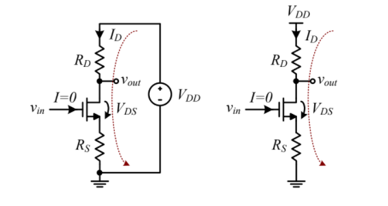
0.2. Kirchoff's Current Law
The sum of all currents flowing into a node is zero $$\sum I = 0$$ $$I_1+I_2+I_3-I_4=0$$
0.3. Resistor Combinations
Resistors in series: Largest resistor dominates $$R_{eq}=R_1+R_2+R_3$$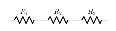
0.4. Voltage and Current Dividers
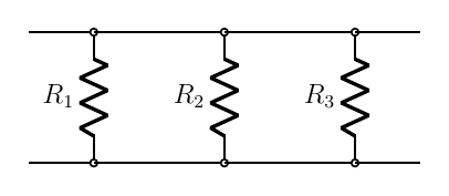
Voltage Divider: The largest resistor takes most of the voltage $$V_{out}=V_{DD}.{R_3 \over {R_1 + R_2 + R_3}}$$

0.5. Thevenin Equivalent Circuit
Any one port circuit can be replaced by a voltage source and a series impedance $$V_{TH}=V_{O.C.}$$1. Mosfet Large & Small Signal Model
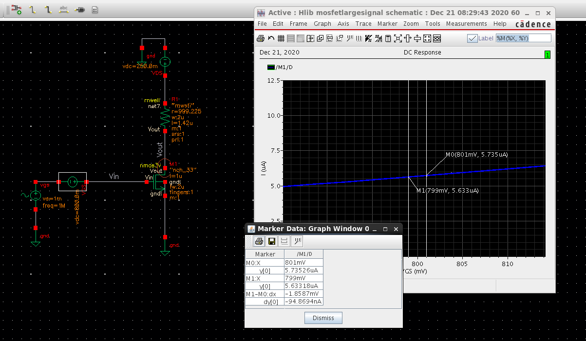
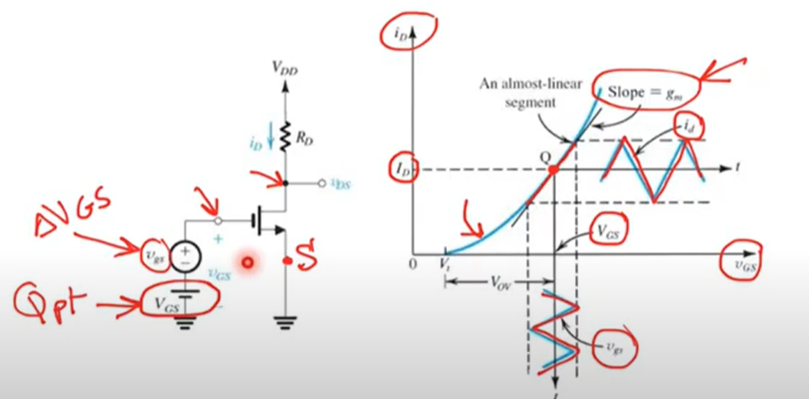
We neglected short channel effect & large VDS effect by using large L=1um and small vds=250mV and we also neglected bodyeffect by grounding the source1.1.Schematic
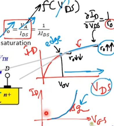
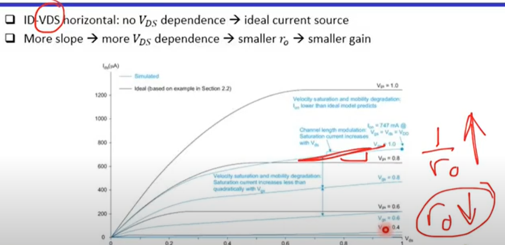
1.2. ID-Vs-VDS

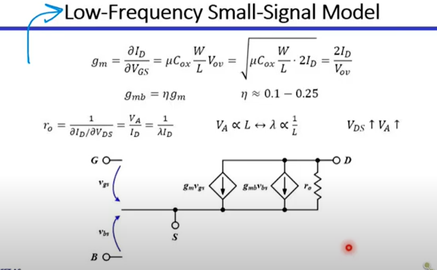
1.3. TransConductance


1.4. Short Channel Effects
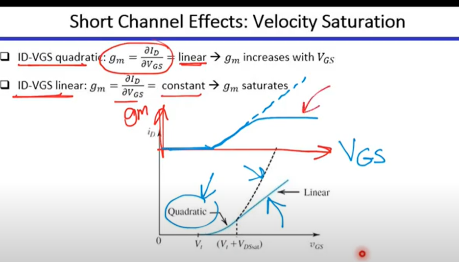
While in case of short channel the relation between mosfet drain current and VGS becomes linear which means that if we drive transconductance we will find that it is of constant value.
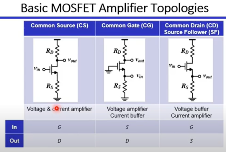
2. Single-Stage Amplifiers
we have three basic amplifier toplogies which are:- Common Source(CS): which acts as Voltage and current amplifier if we inject the signal from the gate and probing on Drain. where source is common between Drain and Gate
- Common Gate(CG): which acts as Voltage amplifier and Current Buffer, Buffer means amplifier of gain=1
- Common Drain(CD) or Source Follower(SF)
- Cascode
| Common-Source Stage | Source Follower | Common-Gate Stage | Cascode |
| with Resistive Load | with Resistive Bias | with Resistive Load | Telescopic |
| with Diode-Connected Load | with Current-Source Bias | with Current-Source Load | Folded |
| with Current-Source Load | |||
| with Active Load | |||
| with Source Degeneration |
2.1. Amplifier Analysis Steps
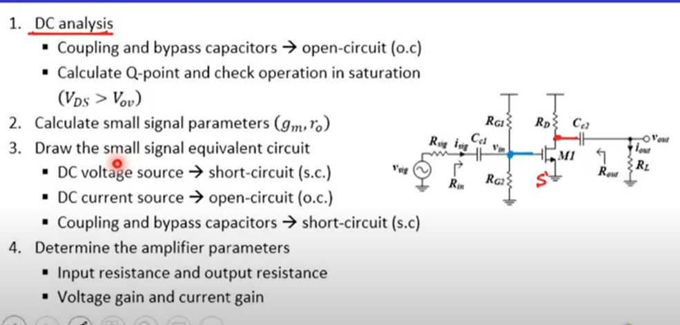
- DC analysis: to calculate DC operating point to check operation of mosfet in saturation (VDS>Vov)
- Calculate small signal parameters(gm,ro)
- Determine Amplifier Parameters(Rin, Rout, Av, Ai)
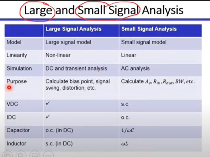
2.1.1. Large Signal Analysis
- Voltage Gain
- Current Gain
- Input Resistance
- Output Resistance
- Bandwidth
2.1.2 Small Signal Analysis
- Bias Point
- Signal Swing
- Distortion
2.1.3. Direct Analysis on Schematic
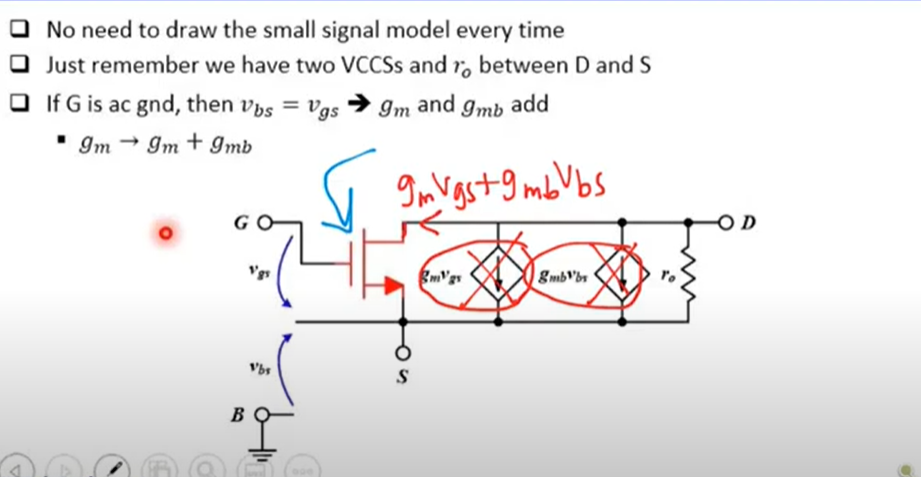
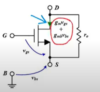
to simplify more, we found that in most cases gate node is grounded when we are calculating small signal model and also we always make the bulk grounded to neglect body effect so that means that Vgs=Vbs so we can gm & gmb together in a single gm so delta_Id=(gm+gmb)delta_Vgs
2.1.4. Common Approximations we usually use:
intrinsic gain >>>1 because it is the max gain we can reach and these approximations are relative for example you can find (1/gm)~=100Kohms which is very large but you will find also that ro=10Mohms thats why I said that approximations are relative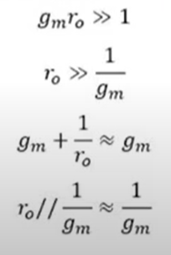
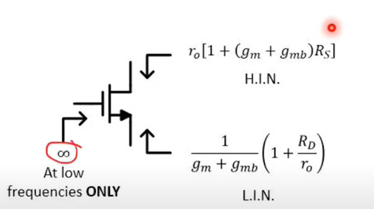
2.1.5. Rin/Rout Shortcuts
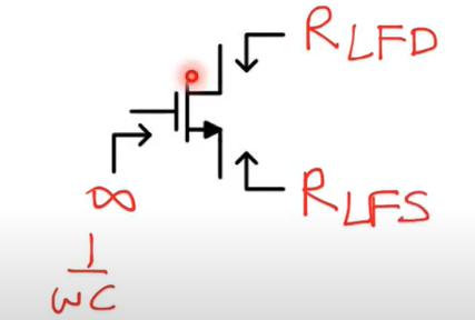
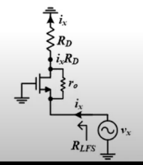
We can simplify the way we use when when we try to find input resistance and output resistance of the amplifier, like as follow in figure below we can focus on three parts:- R_LFS: Resistance when looking from source
- R_LFD: Resistance when looking from drain
- Gate_resistance: is always very large so we doesn't care about calculating it
2.1.5.1. Resistance Looking From Drain
The eye determines the that I want to see output resistance infront of the red vertical line opposite to it, we will find in this case the gate is grounded which means that vgs is only controlled by the voltage drop resistance Rs==>Vgs=-Ix*Rs and we can also neglect body effect as Vgs=Vbs because gate is grounded so we can add gm & gmb to each other while calculating but keep in mind that they are of different values. always try to solve as much as possible on the drawing instead of writting many equations,after all these simplifications we have now only one equation left which is KCL @ node D
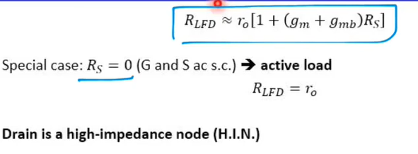
which is:$$i_x ={ (g_m+g_{mb})*(-i_xR_s)+{v_x-i_xR_S \over r_o}}$$ $$R_{LFD}={v_x \over i_x}={r_o+[(gm+gm_b)*r_o+1]R_S}={{r_o}+({g_m}+{g_{mb}}){r_o}R_s+R_s}=r_o[1+(gm+gm_b)R_s]+R_s$$ $$neglecting R_s: then, R_{LFD} \sim = r_o[1+(gm+gm_b)R_s]$$ which can get from it easily Vx/Ix which corresponds to the value of resistance looking from drain we can neglect Rs comparing to gm*ro
we can only put gmb=0 when Rs=0 where we will not have body effect

2.1.5.2. Resistance Looking From Source
when looking from source we have same condition on gate where Vbs=Vgs & delta_Id=gm*delta_Vgs but the voltage on source node will differ because we replaced rs with a voltage source of value Vx and of current Ix which is injected to mosfet so Vgs=Vg-Vs=0-Vx=-Vx and to explain how idrain=isource we can say that mosfet acts like a supernode where by conservation law of charge we can tell that the current that entered this node from the source, it will exit also from drain after all these simplifications what remains now is performing a kcl at source of mosfet.KCl @ node S: $$i_x={(g_m+g_{mb})*v_x}+{ v_x-i_x*R_D \over r_o}$$ $$ R_{LFS}={v_x \over i_x}={1 \over {gm+gmb+{1 \over r_o}}}*{(1+{R_D \over r_o})}= {1 \over {g_m+g_{mb}}}*{(1+ {R_D \over r_o})}$$ $$R_{LFS}={1 \over {g_m+g_{mb}}}*{(1+{R_D \over r_o})}$$ $$ (@RD=0)$$ $$R_{LFS}={1 \over {g_m+g_{mb}}}$$ which means that source acts like low impedance node and this connection @Rd=0 we call it diode connected(gate and drain connected) because @ this case vds=vgs which means that it is now not a voltage controlled current source and changed to a resistor of 1/gm because id=gmvgs=gmvds====>R(diode connected)=Vds/Ids = 1/gm we call it also source absorbtion
in terms of large signal analysis the diode connected mosfet is always at saturation because vds=vgs and the condition for saturation is Vds>Vgs-Vth which will always be satisfied
2.1.5.3. summary
2.2. Voltage Amplifier Model
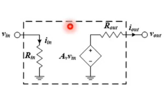
2.2.1. Voltage\Current Amplifier model Equations
Lets summarize these equations as follow: $$R_{in}={v_{in} \over i_{in}}$$ $$R_{out}={v_x \over i_x} @ v_{in}=0$$ $$G_m={i_{out,shortcircuit} \over v_{in}} @v_{out}=0$$ $$A_v={{G_m} R_{out}}$$ $$A_i={{G_m}R_{in}}$$ Remember that we can get first two equations of Rin& Rout from shortcuts that we learned before all remaining will be is calculating transconductance using norton method and then at the end we can get voltage & current gain this method of solution we call it divide and conquer where we simplified large problems into many small problems that we could solve it independent of each other3. Common Source Amplifier
Common Source Amplifier Parameters:
which corresponds to Vsignal.
3.1 Case 1. Rout=Inf. using Ideal Current Source
3.1.1 Theory

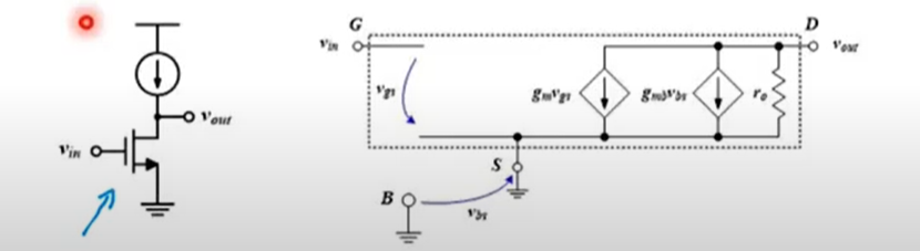
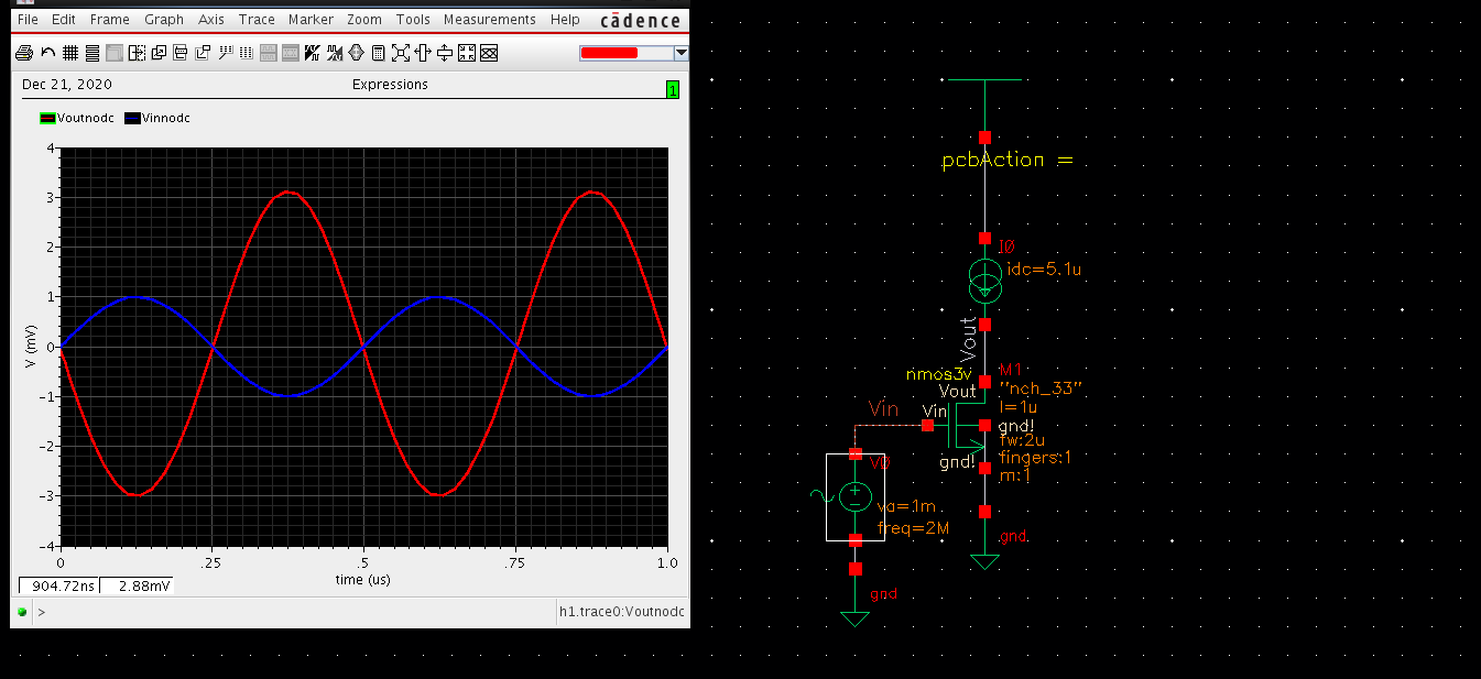
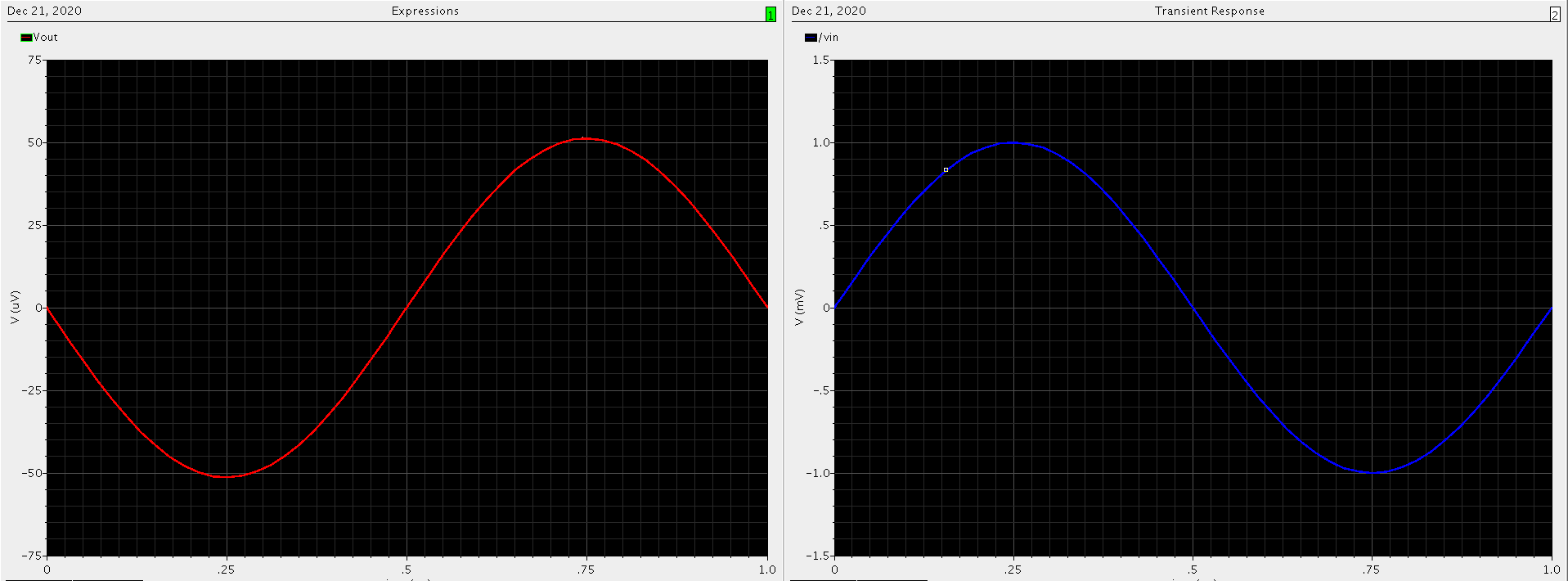
3.1.2 simulation
3.1.3 Hand Analysis
First draw current branch on mosfet drain branch and draw ro in parallel with Vds and vbs connect it to ground away from the circuit as in figure below

3.2 Case 2: using finite drain resistance
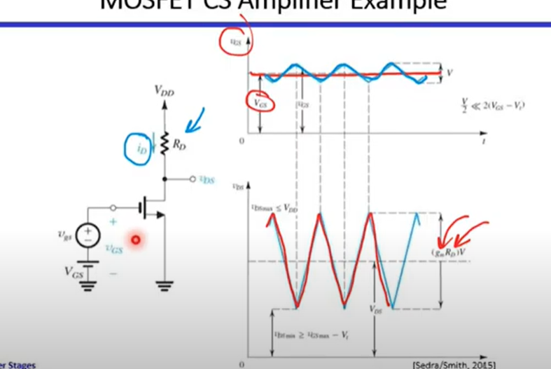
when vgs increases drain current increases which affect vout precedingly as voltage drop on resistance increases which makes Vout decreases thats why they have phase difference of pi==(180 degrees)

3.3. case 3: using finite drain & source resistance
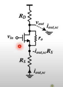
3.3.1. Transconductance
first to calculate transconductance as we said before we will use norton method when we make vout=0(short circuit) as in above figure and calculate iout,sc where now RD will disappear from our calculation because it is parallel with a short circuit and the current will be equivalent to the mosfet drain current where we can get mosfet drain current as follow: $${i_{out,shortcircuit}}={-{g_m}{v_{gs}}+{{v_s} \over {r_o}}}$$ $$and, {v_{gs}}={{v_g}-{v_s}}=v_{in}-v_s$$ $$then,{i_{out,sc}=-g_{m}{(v_{in}-v_s)}+{{v_s} \over {r_o}}}$$ $$and, {v_s}=-{{i_{out,shortcircuit}}Rs}$$ $$then, {i_{out,sc}}=-g_{m}{(v_{in}-(-{{i_{out,sc}}Rs}))+{-{{i_{out,sc}}Rs} \over {r_o}}}$$ $$then, {i_{out,sc}[1+{g_{m}R_s}+{{R_s} \over {r_o}}]}=-{g_m}{v_{in}}$$ $$then, transconductance=G_m={i_{out,sc} \over v_{in}}={-{g_m} \over {[1+{g_{m}R_s}+{{R_s} \over {r_o}}]}}$$3.3.2. Output Resistance
to calculate Rout which is equivalent to thevenin resistance where we will close any independent sources and try to use Rin/Rout shortcuts: $$R_{LFD}=r_{o}[1+(g_{m}+g_{mb})]R_s$$ $$R_{out}={R_{LFD}||R_D}={{R_D}||{{r_o}[1+(g_m+g_{mb})R_s]}}$$ from above equations we could now determine voltage gain and current gain where: $$Voltagegain: A_v={{G_m}{R_{out}}}={{I_{out}\over V_{in}}*{V_{out}\over I_{out}}={V_{out}\over V_{in}}}$$ $$Currentgain: A_i={{G_m}R_{in}}={{I_{out}\over V_{in}}*{V_{in}\over I_{in}}={I_{out}\over I_{in}}}$$3.3.2.1. Output Resistance Cases
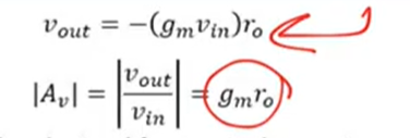
we could have three cases to for RD:- if \(R_D\) is ac o.c.(currentsource): \(A_v=-g_m*ro\)
- if \(R_D <<<< R_{LFD}\): \(A_v=-g_m*R_D\)
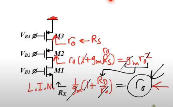
5. Cascode Amplifier
5.1. double stage telescopic cascode with ideal current source as load

5.1.1. Small Signal Analysis
5.1.1.1 TransConductance
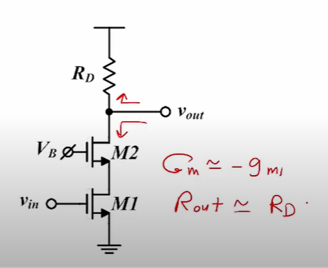
schematic below shows a simple model of cascode amplifier which we will try to calculate its parameters like before as follow(notice that we neglected ro of M1 and remember that common base acts like current buffer): $$i_{out,sc}=-{g_{m1}}v_{in}$$ $$G_{mtotal}={i_{out,sc} \over v_{in}}=-g_{m1}$$ Same Gm of CommonSource amplifier We can solve it also in another way by solving each stage independently like solving first CommonSource stage and try to get inorton you will find it is equal to -gm1 and rout seen from source of M2 as follow: $$i_{norton,Shortcircuit}=-g_{m1}v_{in}$$ $$Transconductance_{firstStage}=-g_{m1}$$ $$i_{norton,shortcircuit}=-g_{m1}v_{in}$$ $$Transconductance_{secondStage}=-g_{m1}$$5.1.1.2. Output Resistance
$$R_{LFDofM1}=ro1$$ $$R_{LFDofM2}=r_{o2}[1+(g_{m2}+g_{mb2}R_{LFDofM1})]$$ $$R_{outtotal}= \infty(currentsource) ||R_{LFDofM2}$$ $$=R_{LFDofM2}=r_{o2}{[1+(g_{m2}+g_{mb2}r_{o1})]} \sim ={(g_{m2}+g_{mb2})}{r_{o1}}{r_{o2}}$$ Rout is significantly boosted by that voltage gain is significantly boosted Second Method: $$R_{LFSofM2}={1 \over {g_m+g_{mb}}}*{(1+{R_D \over r_o})} where R_D= \infty ,so, R_{LFSofM2}=\infty$$ $$OutputResistance_{firststage}=R_{LFSofM2}||r_{o1}=r_{o1}$$ $$R_{LFDofM2}=r_{o2}[1+(g_{m}+g_{mb})]R_s$$ $$where,R_s=0,because, v_{x}=0(Thevenin condition),so,R_{LFDofM2} \sim =r_{o2}$$ $$OutputResistance_{secondstage}=\infty || R_{LFDofM2}=r_{o2}$$5.1.1.3. Voltage Gain
First Method: $$A_v =G_{mtotal} R_{outtotal} \sim = -{g_{m1}(g_{m1}+g_{mb2})r_{o1}r_{o2}}$$ by assuming all gm and ro are equal and neglecting body effect we can get: $$A_v=-(g_m r_o)^2$$ Second Method: $$VoltageGain_{M1}=A_{v1}=G_{m1}*R_{outofm1}=-g{m1}*r{o1}$$ $$VoltageGain_{M2}=A_{v2}=G_{m2}*R_{outofm2}=-g{m1}*r{o2}$$ $$TotalVoltageGain={v{out} \over v_{in}}={v{out} \over v_{x}}*{v{x} \over v_{in}}=A_{v1}*A_{v2}=-(g_m r_o)^2$$5.2. Large Signal Analysis
how Vbias affects the circuit and what do I need from it? first I use it to keep M1 in sat and to keep M1 in sat we need Vds1>Vgs1-Vth1 where the worst case is at the largest value of Vgs because this case will put limits on VB to keep M1 in sat so: $$V_B>V_{GS2}+V_{DS1,max},Where, V_{DS1,max}={V_{overdrive,max}=V_{in,max}-V_{Th1}}$$ $$Then, V_B>V_{GS2}+(V_{in,max}-V_{Th1}) $$ second thing I need from VB is to keep also M2 in sat where: $$to \space keep \space M2 \space in \space sat: V_{DS2}>V_{GS2}-V_{TH2},$$ $$by \space removing \space S_2 \space from \space both \space sides$$ $$\therefore V_{D2}>V_{G2}-V_{Th2}$$ $$where, V_{G2}=V_B, and, V_{D2}=V_{out}, then, V_{out}>{V_B-V{Th2}}$$ $$then, V_B < {V_{out,min}-V_{Th2}}$$ where Vout,min is the minimum voltage required to keep M1,M2 sat which is equal to 2Voverdrive by combining our derived limits we get: $$V_{GS2}+(V_{in,max}-V_{Th1}) < V_B < {V_{out,min}-V_{Th2}}$$ which means that limits on output range is oppositely coupled with input range as condition of Vout,min must be larger than Vin,max + VGS2 for same threshold voltage in order to specify an amount for VB if this doesn't happen we will either hurt input or output range5.2.1. double stage telescopic cascode with finite resistance RD as load
5.3. double stage telescopic cascode with active cascode load
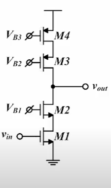
5.3.1. Small Signal Analysis
If we want to keep the large Rout, we must use cascode load why not a current source because in real life there is nothing called ideal current source but we create current source using transistors and why not using single stage because output resistance of the load will be small compared to o/p resistance of the driving cascode so it will act like previous case of using finite RDassuming all gm and ro are equal and neglecting body effect we can get:
$$A_v=-{(g_m r_o)^2 \over 2}$$ we divided by two because Rout seen from the load in this case is equal to Rout seen from the driver in this case so total Rout is equivalent to parallelism of them
5.3.2. Large Signal Analysis
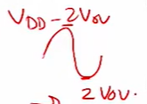
We are concerned about it now because we are now talking about a circuit that can be implemented in real life so we are concerned about biasing the circuit correctly, we now that for every transistor its drain-source voltage must be greater than overdrive voltage so: $$ V_{DSM4}+V_{DSM3}=V_{DD}-V_{SM4}+V_{SM4}-V_{out}=V_{DD}-V{out}>2*V_{ov}$$ $$then, V_{out} <{ 2*V_{ov} }$$ to make M3 & M4 stays in sat region(upper limit)and also: $$ V_{DSM1}+V_{DSM2}=(V_{out}-V_{SM1})+(V_{SM1}-0)=V_{out}>2V_{ov}$$ to make M1 & M2 stays in sat region(lower limit)
and you can remember also the other parameters in large signal analysis by returning in index or you can continue with me we are now concerned with output swing. which we can calculate from upper, lower limits where outputswing=upperlimit-lowerlimit= VDD-4Vov which is demonstrated in figure below:
5.4. double stage Folded cascode with ideal current source as load

5.5. Super Cascode
$$g_{m,super}=A_v * g_m$$ $$r_{o,super}=r_o$$4. Frequency Response
Bode Plot Rules
| Pole | Zero | |
| Magnitude | -20 dB/decade Actual Mag @ pole:-3dB |
+20dB/decade, Actual Mag @ zero: +3dB |
| Phase | \(-90^o\), Actual Phase @ Pole: \(-45^o\) | LHP zero: |